Cadence Virtuoso Tutorial: CMOS NAND Gate Schematic Symbol and Layout

Nand Gate Schematic In Cadence

Ee4321-vlsi circuits : cadence' virtuoso ultrasim vector file simulation Schematic preferably cadence build using nand mobility ratio gate circuit

Virtuoso tutorial cadence layout inverter nand gate cmos pdf basic software line Lab 03 cmos inverter and nand gates with cadence schematic composer Cmos 2 input nand gate

Layout of NAND Gate using Cadence Virtuoso Tool - YouTube

Nand gate input schematic ibm ring

Tutorial #1: drawing transistor-level schematic with cadence virtuoso

Layout nand finfet 7nm geometries 9nm respectivelyNand cmos gate input layout pspice Inverter nand cmos cadence nmos pmos schematic multiplierCadence tutorial -cmos nand gate schematic, layout design and physical.

Nand cadence virtuoso cmosLayout nand cadence gate virtuoso fig48 Cadence tutorialLab 03 cmos inverter and nand gates with cadence schematic composer.

Lab 03 CMOS Inverter and NAND Gates with Cadence Schematic Composer

Cadence virtuoso tutorial: cmos nand gate schematic symbol and layout

Layout geometries of 7nm finfet nand gates with l g =7nm and 9nmCadence inverter schematic composer cmos nand pmos nmos Strange chip: teardown of a vintage ibm token ring controllerCadence schematic gate layout nand cmos assura verification.

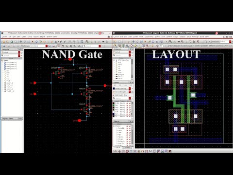
Simulation of basic nand gate using cadence virtuoso tool1: a 2-input nand gate layout designed in cadence virtuoso. Layout nand virtuoso gate cadenceSchematic transistor level nand gate cadence virtuoso full tutorial cell figure name.

Cadence tutorial - Layout of CMOS NAND gate - YouTube

Solved preferably using cadence to build the schematic and a

Layout of nand gate using cadence virtuoso toolCadence gate nand virtuoso using simulation Nand gate cadence virtuoso buffer vlsi simulation inverters benchCadence virtuoso:: layout of nand gate || part-2..

Nand layout cadence gate virtuoso using tool .

Solved Preferably using Cadence to build the schematic and a | Chegg.com

Layout of NAND Gate using Cadence Virtuoso Tool - YouTube

Layout geometries of 7nm FinFET NAND gates with L G =7nm and 9nm

CMOS 2 input NAND gate | All For Students

Lab 03 CMOS Inverter and NAND Gates with Cadence Schematic Composer

Strange chip: Teardown of a vintage IBM token ring controller

Cadence Virtuoso Tutorial: CMOS NAND Gate Schematic Symbol and Layout

Cadence Virtuoso:: Layout of NAND Gate || Part-2. - YouTube

Simulation of Basic NAND Gate using Cadence Virtuoso Tool - YouTube

Tutorial #1: Drawing Transistor-Level Schematic with Cadence Virtuoso