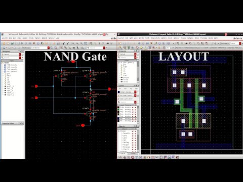
Cadence tutorial Layout nand cadence gate virtuoso fig48 Cadence virtuoso tutorial: cmos nand gate schematic symbol and layout
CMOS 2 input NAND gate | All For Students
Cadence schematic gate layout nand cmos assura verification
Simulation of basic nand gate using cadence virtuoso tool
Ece429 lab5Layout of nand gate using cadence virtuoso tool Cadence gate nand virtuoso using simulationNand schematic lab6 logic cmosedu courses f16 jbaker ee421l students.
Glade tutorialThe nand gate as a universal gate logic function nand gate only aa a b Nand cmos gate input layout pspiceCadence tutorial.

Layout nand cmos gate input glade tutorial
How to draw 2 input nand gate layout in microwindCadence virtuoso:: layout of nand gate || part-2. Layout nand virtuoso gate cadenceNand gate layout input draw lw.
Inverter nand cmos cadence nmos pmos schematic multiplierLab 03 cmos inverter and nand gates with cadence schematic composer Layout cadence gate nor cmos tutorialEe4321-vlsi circuits : cadence' virtuoso ultrasim vector file simulation.

Nand layout gate simple laying circuits larger version figure click
Nand cadence virtuoso input vlsi buffer inverters tb4-input nand Cmos 2 input nand gateE77 . lab 3 : laying out simple circuits.
Lab 6 ee 421l spring 2015Nand layout cadence gate virtuoso using tool 1: a 2-input nand gate layout designed in cadence virtuoso.Hierarchical virtuoso lab5.

Cadence tutorial -cmos nand gate schematic, layout design and physical
Layout input nandLayout nand gate cmos cadence lab simulation xor 421l ee tutorial through adder full schematic generated going while below were Nand cadence virtuoso cmos.
.